

A 180° ring-shaped LED module does not necessarily have to be made as one 180° PCB.
In one NKT prototype project, the customer required a 180° ring-shaped LED module. Producing the complete 180° section as a single PCB was technically possible, but the PCB cost was substantially higher.
The reason was related to the geometry itself. A large curved PCB requires a board area large enough to accommodate its complete outline. Much of that area may not remain in the finished ring-shaped PCB.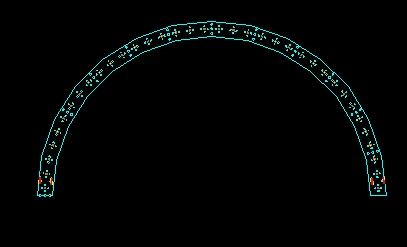
Instead, we divided the design into four identical 45° curved PCBs. Together, the four sections formed the required 180° module while allowing the PCB material to be used more efficiently.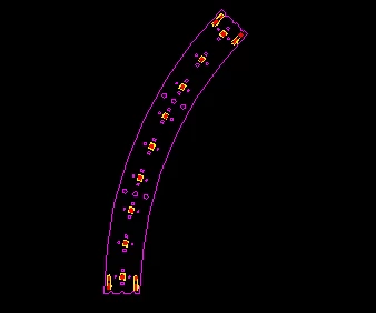
This project illustrates an important point in custom LED module development:
PCB shape does more than define the outside edge of the module. It defines the usable space for the LED layout and, in some projects, can even influence whether the final module is produced as one PCB or several repeated PCB sections.
PCB Shape Starts With the Customer's Application
At NKT, PCB shape is determined by the customer's application rather than selected independently.
Sometimes the customer provides the PCB dimensions and outline directly. In other projects, the available product or housing space provides the mechanical boundary from which the PCB design is developed.
The information available at the beginning also varies.
Some customers already specify an LED model. Some provide a target lumen output. Others may already have more of the module design defined.
Once the application geometry is known, however, the available PCB area becomes one of the boundaries for the LED layout.
The useful question is therefore not simply:
Is the PCB round, ring-shaped or linear?
It is:
How much usable layout area does that geometry leave for the required LED quantity and arrangement?
A Round PCB and a Ring PCB Do Not Provide the Same Usable Area
A full round PCB allows LEDs to be distributed across the circular board area, subject to the other mechanical requirements of the project.
A ring-shaped PCB changes that immediately because the center is no longer available for LED placement.
NKT has produced complete ring-shaped PCBs, including designs with multiple concentric rows of LEDs. The actual arrangement depends on the ring dimensions, LED package, required LED quantity and the requirements of the particular module.
The important difference is not that a ring PCB requires one specific LED pattern.
It is that the required LEDs have to fit within the remaining annular area.
This becomes particularly relevant when the customer has a fixed outer diameter and a required light output. Removing the center reduces the available layout space, but the required LED quantity and circuit still have to work within the remaining ring.
This is one reason LED quantity needs to be considered together with PCB area and electrical configuration rather than being selected independently.
Linear PCBs Have a Different Geometric Constraint
On a linear PCB, NKT generally arranges the LEDs as evenly as practical along the available board length.
We have produced both single-row and double-row linear LED PCBs.
Whether a project uses one row or two is not determined by a fixed rule for linear modules. It depends on the available width, LED quantity, spacing and the requirements of the particular application.
For example, a project may require higher output while the PCB remains narrow. There may be enough length available, but the board width can limit how the additional LEDs are arranged.
In this situation, the linear shape itself does not necessarily create a special electrical problem.
The geometry-related question is more straightforward:
Can the required LED arrangement fit within the available length and width?
If not, the design variables have to be reconsidered within the customer's actual product constraints rather than forcing a standard LED pattern onto the board.
Sometimes Geometry Also Affects Whether the PCB Should Be Divided
The 180° ring project introduced another design decision.
The required final geometry was already clear: the customer needed a 180° ring-shaped LED module.
Making the complete 180° section as one PCB was technically feasible.
However, PCB cost is not simply determined by looking at the amount of material that remains in the finished curved board. For this type of large ring-shaped PCB, the board area needed to accommodate the complete curved outline can be much larger than the area visible in the finished PCB.
In this project, the quotation for the complete 180° PCB was substantially higher.
So we kept the customer's required final geometry but changed how the PCB was divided:
180° final module = 4 identical 45° curved PCBs
Because all four PCB sections were identical, the same LED layout and design parameters could be repeated across the four sections. When assembled together, they created the required 180° ring.
The smaller curved sections allowed the PCB material to be used more efficiently and significantly reduced the PCB cost for this project.
This does not mean that every large ring-shaped or curved LED module should be divided into smaller PCBs. NKT also produces complete ring-shaped boards, and the appropriate approach depends on the specific module dimensions, design requirements and PCB manufacturing conditions.
The practical lesson from this project is narrower:
When a custom PCB has a large curved or unusual outline, it can be worth evaluating not only the LED layout, but also whether the required final geometry needs to be produced as one PCB.
This particular project remained at the prototype stage and did not proceed to volume production.
PCB Geometry and Local Mechanical Constraints Are Different Questions
The overall PCB shape is only the first mechanical boundary.
Even after that shape is defined, mounting holes, connectors and other mechanical constraints can further affect the usable LED layout area.
For example, a round PCB may provide sufficient total area for the required LED quantity, but a mounting hole located at a preferred LED position can still force the layout to change.
That is a different problem from the overall PCB geometry discussed in this article.
PCB shape defines the overall layout region. Mounting holes, connectors and other local constraints determine how that region can actually be used.
Keeping these two questions separate makes it easier to understand why an LED layout changes.
Start With the Product, Not a Standard LED Pattern
There is no single correct LED pattern for every round, ring or linear PCB.
Two modules with similar outside dimensions may require different layouts because the LED model, target output, available space or other application requirements are different.
That is why the starting information for an NKT project is not always identical.
A customer may already have the PCB dimensions and LED model. Another may have the mechanical space and a target lumen output. Some customers may already have much more of the design defined.
The module therefore has to be developed from the project information that is actually known rather than from a standard LED pattern.
A practical way to view the process is:
Customer application → PCB geometry → usable layout area → LED quantity and arrangement → circuit layout → prototype validation
Some of these parameters may already be fixed when a project reaches NKT, but the underlying principle remains the same:
The LED layout has to work within the customer's product geometry—not the other way around.
For OEM products where a standard LED board cannot meet the required dimensions, layout or performance, NKT develops custom OEM LED modules around the customer's actual product and application requirements.
Need an LED Module Designed Around Your Product Geometry?
If your product already has defined dimensions, mounting space or PCB geometry, NKT can develop the LED module around those application requirements.
Send us the dimensions, drawings, LED requirements, target light output or other project information you already have. Not every specification needs to be finalized before the initial review.